Lab 7: Reactive Nodes
Overview of Lab
In this lab you will create three separate embedded programs and a node-red configuration to interact with them. The first two programs are tutorial in nature – in “button” you will learn how to connect an external signal, a button, to an interrupt in order to alert the processor of external events. In the second program, adc, you will learn about the conversion from analog sensors to digital values and, equally important, about the need for calibration with “real sensors”. Finally, you will combine what you have learned to build an IoT node that interacts, with Node-Red and, through Node-Red, with the Flespi MQTT account you created in a previous lab.
As before, your report should document your efforts and describe any code that you created. The report does not need to be verbose, but should be a coherent snapshot of your work and any difficulties/issues that arose.
The grading rubric for this lab is
- Completion of tasks 60%
- button : 10%
- adc : 10%
- react : 20%
- node-red flows/dashboard : 20%
- Lab report 40%
- summary : 5%
- discussion of tasks : 10%
- discussion of your code/flows : 20%
- issues : 5%
Deliverables
The specific deliverables are:
- button – you will modify the starter code to make it interrupt driven
- adc – you will modify the starter code to handle calibration and temperature calculation
- react-node – you will build an “iot node” using components from 1 and 2 consisting of two parts
- an embedded program (call this react)
- a node-red flow connecting react with flespi and a node-red control panel
- Report.md – your report
Organization of lab7 directory
You should start by copying the lab7 directory from lab-instructions/labs/lab7 to labs/lab7 in your repo. This
directory is organized as follows (the lower level src directories are not expanded in this view):
├── adc
│   ├── makefile
│   ├── project.mk
│   └── src
├── button
│   ├── makefile
│   ├── project.mk
│   └── src
├── cfg
│   ├── chconf.h
│   ├── halconf.h
│   └── mcuconf.h
├── inc
│   └── react.h
├── make.mk
└── src
    ├── adc.c
    ├── message.c
Because the goal of this lab is somewhat more complicated than previous labs, some code – message.c
and adc.c has been moved to a “global” directory along with a shared include file react.h.
The project.mk file provides the necessary project specific declarations by defining:
- the path to any “include” files you might create
- a list of the source files to include in building the project
1. Building and Executing a Button Monitor
In this part of the lab you will learn how to monitor an external signal – the blue “user button” on your nucleo board to determine when it changes state (pressed/open). You have been given a “starter” program that monitors the button state with polling – literally repeatedly reading the button state and waiting. After you have tested this program, you will be led through the process of converting this program to use interrupts in order to reduce the overhead required for polling and improve the program’s response to button “events”.
1.1 About Buttons
The stm32l476 nucleo board has two buttons – a black one that will reset the processor and a blue, “user”, button that is available for applications. The blue button is connected, with a small amount of electronics (discussed below), to pin PC13 on the stm32l476 processor. When the button is pressed, the pin is “pulled” to 0, and when the button is released, the pin is “pulled” to (logical) 1.
The following discussion is not necessary to accomplish this laboratory assignment, but may be of interest to students who want to understand a bit about the physical design of sensor nodes. As mentioned above, the button is connected to processor pin PC13 along with a small number of electronic components. This is illustrated in the following circuit fragment from the stm32l476rg nucleo user’s manual:

In this circuit, the button (labeled) B1 is shown as “normally open”. The actual button device has four pins – 2 and 3 are connected to PC13, and 1 and 4 are connected to “ground”. PC13 is pulled high (to VDD) through a resistor (R30). Capacitor C15 and R30 together form a simple “filter” to eliminate electrical bounce when the button is pressed or released. Resistor R29 serves as a current limiter when the capacitor is discharged. To understand the need for these additional components, consider the following figure that captures the signal when an unfiltered button is pressed:

The problem is that the mechanical contacts that form the switch vibrate slightly when the button is pressed or released causing the connection to be made and broken repeatedly as the switch settles. The role of the filter elements is to electronically remove these brief (rapid) signals. Consider the signal when a filtered button is pressed (the filter circuit was somewhat different in this example, but still a capacitor and resistor).

Notice that all of the “bounce” has been eleminated.
1.2 The “button program”
In this part of the lab, you are given, as a starting point, a program that determines the state of the user button by reading pin PC13. The starter code creates a thread, called “button” that executes the following loop:
|
|
The basic logic is, every 200msec, the thread wakes, reads the button pin (line 3), and sets the green led on or off accordingly if the “state” of the button has changed since the last iteration. In this example, the state is determined by reading the LED pin (lines 4,7). ChibiOS abstracts away many of the details for reading/writing pin values. Diving a bit deeper into line 3, the pin naming scheme for stm32 is (port, number). In this case, port C (GPIOC) and pin 13. It is common for embedded processors to organize blocks of pins into so-called “ports”. At the lowest level all of the pins in a port may be read or written in parallel.
Because the code you will be writing will utilize the serial port from multiple threads,
the chprintf function has been abstracted in the message.c module. In particular,
any shared resources are protected by mutexes.
Your first task is to build, download, and execute this program. You can see the text output using the “goshell” program used and discussed in Lab 6. In addition, you should be able to see the button state reflected on the green led.
When you run the program try
- Pressing and releasing the button with a delay
- Try tapping the button quickly
- Typing a string in the shell – it should be echoed
You should notice that it is possible to tap the button and not see the light blink. While there may be cases where this is desired, in general a user would expect even a brief tap to have an effect – think about the buttons on a mouse.
The underlying problem is the architecture of this program – it “sleeps” between readings of the button input. We could ameliorate the “missed tap” problem by shortening the delay, but only by spending more of the processor’s time simply executing this read loop. The fundamental solution is to “tie” the button to an interrupt and to arrange for the button thread to sleep between interrupt events.
1.3 Interrupt Driven Button Program
As discussed in lecture, an interrupt source is an external or internal device that can alert the processor to an interesting event. When an (enabled) interrupt event occurs, the processor transfers control to an associated interrupt “handler” – really a special procedure – that determines the appropriate action to take.
The process of enabling interrupts and designing interrupt handlers can be complex and is certainly daunting for many programmers. Fortunately, ChibiOS provides a way to abstract much of this away for the common cases – such a responding to an event on a processor pin.
Your task is then to convert the button program into an interrupt driven program. This requires very modest changes to the button thread code. Before entering the main loop, the button thread must enable the appropriate interrupt:
palEnablePadEvent(GPIOC, 13U, PAL_EVENT_MODE_BOTH_EDGES);This line of code enables the interrupt for PC13 if its input changes (in either direction). It is also possible to detect only low-to-high transitions (PAL_EVENT_MODE_RISING) and high-to-low transitions (PAL_EVENT_MODE_FALLING).
Rather than poll the pins, we can modify the program to wait for an interrupt event rather than waiting for the passage of time:
palWaitPadTimeout(GPIOC, 13U, TIME_INFINITE);This command takes an extra “timeout” argument that is useful in other contexts – here we choose to wait forever. Convert the button program to use interrupt events and test it as before. Note any changes in behavior in your lab report.
2. Analog to Digital Conversion – Temperature Sensor
Most sensors that you are likely to encounter produce, as their output, either an analog signal (a voltage) or a digitized analog signal. Thus, with most sensors a key processing step involves the
conversion of a voltage to a number. In this section, you will build a program that utilizes the
analog to digital converter (ADC) of the stm32 to “read” the value of the temperature sensor on the
processor chip. Because this sensor measures the temperature of the silicon die, and the processor
execution generates heat, it is a poor sensor to use for measuring ambient temperature. However,
it is a good way to understand the process of measuring analog signals as well as some of the technicalities that affect sensor accuracy. In the next lab you will begin to use sensors external to the stm32 that provide their own analog to digital conversion.
2.1 General Background
At the heart of many ADCs lies a digital to analog converter (DAC). The simplest DAC architecture is a so-called binary weighted resistor. As illustrated in the following figure (source)

A binary input –
$$ B_1B_{2}...B_{N} $$
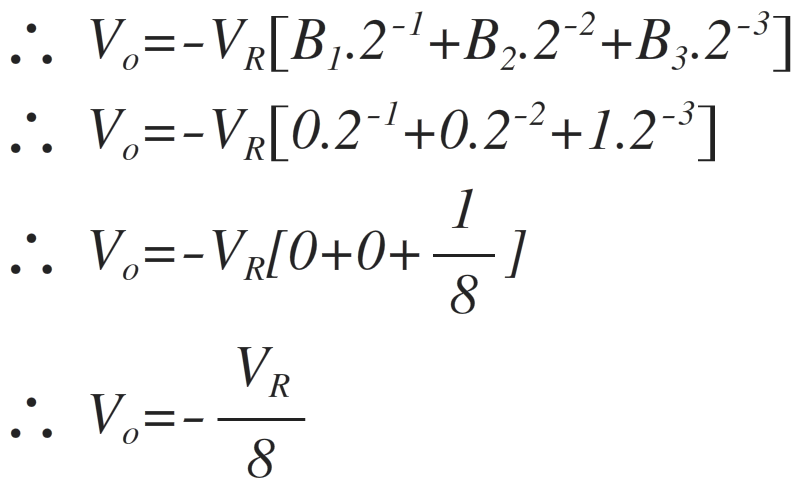
controls a set of switches that connect a reference voltage to an output amplifier through a set of weighted resistors. Given the relative resistances shown, the output voltage is:$$ V_O = - V_R * (B_1*2^{-1} + B_2*2^{-2}... B_N*2^{-N}) $$
Practical DACs are somewhat more complicated, but the basic principle is the same – given a reference voltage, the DAC creates an output voltage that is a binary fraction of the reference voltage.
To create an ADC from a DAC, two additional components are needed – a sample-and-hold circuit, which can capture an input voltage by charging a capacitor, and a voltage comparator, which produces a “high” or “low” voltage depending upon which input has the greater voltage. A typical sample and hold circuit has the following structure:

To sample the input a switch is closed and a capacitor is charged. After a suitable sampling interval, the switch is opened and the capacitor voltage, which is buffered, can be measured. The measurement is performed by comparing the sampled-voltage to the output of a DAC as illustrated:

The ADC Control “searches” for a solution by testing various values of DR. By performing a binary search, an N-bit conversion can be performed in N steps.
There are three important takeaways from this discussion
- Analog to digital conversion takes time
- The output number is a binary fraction of the reference voltage
- In order to measure the voltage of a signal, you have to know the reference voltage
2.2 The stm32 ADC
The stm32 ADC works largely as described above except that the reference voltage depends upon the processor supply voltage, which is implementation dependent, and, most importantly, it is controlled by a complex state-machine that makes it possible to measure a variety of of external (pins) and internal sources in a timer controlled sequence. In order to compensate for the fact that the reference voltage is not a known constant, one of the internal sources is a so-called band-gap reference (Vref) that produces a known voltage. By measuring Vref, and given the solution at a known calibration voltage, we can compute the V_R (in the equation above V_O becomes the known and V_R, the unknown) – more on this below.
There are two further complications. Both Vref and the temperature sensor are sensitive to manufacturing tolerances – even across a single wafer. Therefore, the each is calibrated at manufacturing time given known voltage and temperature; this calibration process results in constants that are stored in the memory of the chip in the form of the binary numbers that were measured by using the ADC at these known voltage and temperature. There is a single constant that can be used to compute V_R and a pair of constants – measurements at two different temperatures – that define the linear voltage to temperature conversion. Don’t panic – this will be explained in further detail below.
As mentioned previously, the stm32 includes an internal temperature sensor which produces a temperature dependent voltage. The process of using this temperature sensor is then:
- Measure Vref
- Compute V_R using calibration data.
- Measure the Temperature sensor
- Scale the Temperature sensor measurement by V_calibration/V_R
- Compute the temperature using calibration data
Consider the question of determining the processor voltage (V_R) first. As mentioned, the stm32 has a built-in voltage reference source – a so-called “bandgap” reference which is an analog circuit that depends upon semiconductor physics to generate a known voltage that is (relatively) stable across temperature (if you are interested, you can read more here). While the bandgap circuit is relatively stable, the voltage it produces may vary (a lot) between components. This problem is handled in manufacturing either by using lasers to “trim” the circuit, or, in the case of the stm32 by storing a so-called calibration constant in memory during the manufacturing process. The following figure taken from the stm32l476 data-sheet illustrates the magnitude of the problem:

The three curves illustrate the behavior of the typical and worst-case (min,max) voltage references in acceptable processors. Notice that each of the curves shows about 0.5% variation over temperature, but the variation between the min/max cases is around 4%. As mentioned above, the solution, in the case of the stm32, is to store a calibration constant in memory. This calibration constant is the actual binary reading taken from converting the voltage reference with the adc at a known voltage.
2.3 Computing V_R
For the stm32l476, this calibration constant is stored as follows
const uint16_t *VREF_CAL = ((uint16_t *) 0x1FFF75AA);and the calibration voltage is 3.0 volts. We can compute V_R using this constant as follows. Suppose that VREF_MEAS is
the adc measurement taken with an unknown V_R, and MAX_MEAS is the “full range” of the adc, then the following equation
defines the relationship between V_R and 3.0 volts:
V_R * VREF_MEAS/MAX_MEAS == 3.0 * (*VREF_CAL)/MAX_MEAS
V_R/3.0 == (*VREF_CAL)/VREF_MEAS
The stm32l476 provides more detailed specifications of the voltage reference:

2.4 Computing Temperature
The temperature sensor in the stm32 also requires calibration. There are two calibration constants which are the (binary) measurements of the sensor taken at 30 and 110 degrees celsius with a 3.0V supply. The These two constants define a line – as illustrated in the following graph

We can convert this into a normal line equation of the form y = m*x + b which will allow us
to compute the temperature (y) for a (scaled) temperature (x). We can deterine m and b as follows:
m = ((float)(110-30))/(CAL2 - CAL1)
30 = m*CAL1 + b
b = 30 - m*CAL1
Given an adc measurement of the temperature sensor Tmeas, we can then compute the temperature as follows:
T = m * (Tmeas * V_R/3.0) + b2.5 Creating your ADC program
The sample code provided does everything except compute the processor V_R (called vdd in the program) and the temperature. Your task is to modify this code to perform the necessary computations. Start with getting the correct system voltage calculation – this should be about 3.3V. Once that is working, get the temperature calculation working in two stages – first make sure the measured voltage of the sensor makes “sense”; then compute the temperature.
The adc code that you need to modify is in lab7/src/adc.c. There are comments illustrating
where your code should go.
The following table defines the behavior of the sensor
At 30 degrees, the measured voltage of the temperature sensor is in the range 0.74-0.78 volts. The “slope” of the
sensor is about 2.5mv/degree. While room temperature is around 21 degrees C, the temperature sensor is on the processor die which is heated by the energy dissipated. If we assume the die temperature is around 25 degrees, the temperature sensor should be in the range 0.72-0.8 volts. (To compute the voltage, voltage = vdd * tmeas/4095).
Do not expect the temperature to be exactly correct. The sensor itself is only accurate to 1-2 degrees even before considering die heating.
3. React Program (Embedded)
For this portion of the lab, you are not given any starter code; rather, you will adapt code from this and previous labs. Start by copying the button directory to a “react” directory at the same level. You will be reusing parts of the button and adc examples for this portion of the lab.
You should create an embedded program that has the following specification
- The node generates messages, both internally and in response to received commands
- All generated messages will be of the form
Node/status/topic valuewhere the topics are- button
[up/down](e.g.Node/status/button up) - temperature
[float](e.g.Node/status/temperature 21.5) - voltage
[float] - led
[on|off]
- button
- All received messages will be of the form
Node/read/topicorNode/write/topic value- read/button (e.g.
Node/read/button) - read/voltage
- read/temperature
- read/led
- write/led [on|off]
- read/button (e.g.
- All generated messages will be of the form
- The node has three threads
- button – responds to button events and sends a status message when the button state changes
- adc – every 30 seconds, sends two status messages – voltage and temperature – and updates local “caches” of these values.
- main – parses input messages and responds to read/write requests by reading the current led/button values or cached voltage/temperature values and writing to the led.
To facilitate the creation of this more complex project, the code for the serial port and the adc were separated out. Your button program should serve as a good starting point (with the addition of a thread to read the adc at regular intervals.)
Most of the code you need is from the previous two examples along with the shell you created in the previous lab.
One complication to this code is that the output device (SD2) is used by more than one thread. Reading
the button from two threads isn’t a problem, but accessing the output device is. Rather than have the
main thread read the adc, the adc thread should “cache” temperature and voltage in global variables
that the main thread can read. The SD2 input and output is “protected” by a pair mutex
of mutexes (in lab7/src/message.c).
You can read the current state of the button and led as follows:
palReadLine(LINE_LED_GREEN)palReadLine(LINE_BUTTON)You can force a thread to sleep for some period (e.g. 1⁄2 second) with
chThdSleepMilliseconds(500)For long sleep periods (e.g. more that 30 seconds) there are other techniques that must be used.
Test your program thoroughly using the goshell
4. Node-red
Once you have created and tested your embedded code with goshell, create a node-red
flow to communicate with the embedded code. At this stage, don’t worry about
communicating with a dashboard. Your goal is simply to
understand how to interface with your Nucleo board, send it commands, and capture output from your board with debug nodes.
In the next section, you will be expanding your node-red flow to talk to an mqtt server. In order to simplify the transition, it’s helpful if all messages within the flow are of the form “{“topic” : “some topic”, “payload” : “some payload”}. Since the board “talks” strings, we’ll have to do some converting.
- on input from the serial port (board) you’ll need to convert from strings to messages
- on output to the serial port you’ll need to convert from messages to strings
In addition, in the next section you’ll need to be able to select messages from the mqtt server that are destined from your board. To illustrate these ideas, consider the following flow (which communicates with an mqtt server, but not a serial port). Note: this example is just to explain some important ideas.

Starting from the left:
- The top three inject nodes model commands for the nucleo board. These have the topic/payload form
- the fourth inject node models status from the nucleo board. This has a string payload
In the center are three filters.
string-to-msgconverts a string to a topic/payload formNode/statussimply passes on topic/payload messages where the topic is of the formNode/status/#Node/read|writefilters out commands to the nucleo and converts them to string form.
The javascript for the string-to-msg filter is:
var str = msg.payload.split(" ")
msg.topic = str[0]
msg.payload = str.slice(1).join(" ")
return msg;
Notice that it splits the payload on the first space and assigns the two parts to topic/payload respectively.
The javascript for the “Node/status” filter is:
if (msg.topic.startsWith("Node/status")) {
     return msg;
}
This code looks for messages with the correct form Node/status/... and passes those through.
Finally, the Node/read|write filter looks for commands to the Nucleo and reformats those as strings:
if (msg.topic.startsWith("Node/read/") ||
    msg.topic.startsWith("Node/write/")) {
    msg.payload = msg.topic + " " + msg.payload;
    msg.topic = "";
    return msg;
}
To build your flow, replace the From Nucleo inject node with a serial port input; add a serial
port output to the output of Node/read/write. Initially, leave out the mqtt nodes and just
connect all of the input wires to the output wires. In the next section you’ll use your flespi
account to communicate with your Nucleo node and a dashboard. Alternatively, you could start by communicating with a local mosquitto server (you’ll have to start one up as described in the MQTT lab).
I don’t recommend using one of the “public” servers since your messages will collide with those of your
classmates.
5. Node-red/flespi/dashboard
Once you have tested a skeleton node-red flow, it’s time to build a real “app” where
- Messages from the embedded node are sent to your flespi account
- read/write messages from your flespi account are sent to your embedded node
- read/write messages can be generated from flow inject nodes and these are forwarded to your flespi account
- status messages from your flespi account are also displayed on a node-red dashboard.
The dashboard should display:
- the current voltage and temperature with gauges
- the button state in a text box
- controls the led with a pair of buttons
- Led off
- Led on